Real Time Geolocation and Weather Device “Citadel”

By Tyler Bovenzi
Initial Ideas
Concept
The purpose of this project is to create a custom real time geolocation and condition reporting device. This device should be self contained on a printed circuit board with the option to connect auxiliary chargers, batteries and antenna. Such a device should report sensor recordings remotely, such that they can be viewed on a webpage or remote terminal. Ideally, software changes can also be made remotely while the device is being used in the field to allow dynamic usability.
The final version of this device will consist primarily of small form factor, surface mount components, as to minimize the footprint. These components should be inexpensive, easy to replace, and well documented for future integrations.
Power should be delivered by an attached rechargeable battery. The board will also host a regulated auxiliary power input to permit integration with solar cells or other sources in the field. Local communication and charging will be facilitated through an onboard universal connector, such as micro USB or USB type C.
Desired Features
There were a host of features I wanted the final version of the project to have:
- Weather
- Pressure
- Humidity
- Temperature
- Air Quality Monitoring
- TVOC
- CO2
- Cellular Communication
- Geopositioning data
- Status Indication
- Power management
- GPIO Expansion
- Auxiliary Antenna Support
Integrated Technologies
Integrated Circuits
- BME280 Temperature, Pressure, Humidity
- CCS811 Air Quality Index
- SAM M8Q Global Positioning System
- Particle E Series Microcontroller, Power Management, Cellular
Additional Components
- 2000mAh 3.7V Lithium Polymer Battery
- Coin Cell Battery for GPS persistent power
- Penta Band Cellular Antenna
- Status Indicating LEDs
- Green, Blue, RGB
- Assorted Resistors and Capacitors
- Mode Push buttons
Bill of Materials
| Part | Cost | Number | Net |
| USB C | $2.50 | 1 | $2.50 |
| BME280 | $6.55 | 1 | $6.55 |
| CCS811 | $12.80 | 1 | $12.80 |
| SAM_M8Q | $25.00 | 1 | $25.00 |
| JST | $0.58 | 1 | $0.58 |
| RGB | $0.19 | 1 | $0.19 |
| CoinCell | $1.75 | 1 | $1.75 |
| 1k resistor array | $0.40 | 2 | $0.80 |
| Green LED | $0.22 | 1 | $0.22 |
| Blue LED | $0.18 | 2 | $0.36 |
| E Series/Ant/Bat | $82.62 | 1 | $82.62 |
| 1.0uf cap | 0.38 | 2 | 0.76 |
| 22 res | 0.1 | 2 | 0.2 |
| 2.2k res | 0.1 | 2 | 0.2 |
| 100k res | 0.1 | 1 | 0.1 |
| 4.7k res | 0.35 | 1 | 0.35 |
| 3.3k res | 0.035 | 1 | 0.035 |
| button | 0.21 | 2 | 0.42 |
| diode | 0.41 | 1 | 0.41 |
| Total | $135.44 |
Additional Expenses
- PCB manufacturing: JLCPCB
- Cheaper than OshPark, similar manufacture time
- Assorted Components: Digikey
- Extensive component inventory
- Specialty Connectors: Sparkfun
- Abundant Documentation
- Microcontroller, Antenna, Battery: Particle
- Shipping: DHL, FedEx, UPS
Schematic
Schematic Design
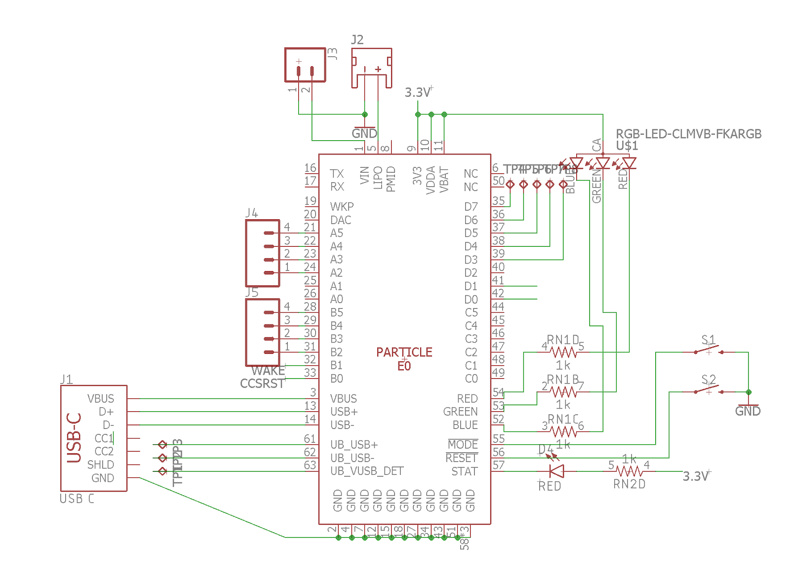
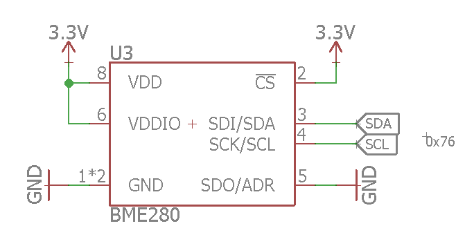
After researching the components I planned on using, I began laying out the design as an electrical schematic. After pouring through extensive datasheets, I learned the pinout of each component. I then decided on how to interface them and handle communication protocols. The GPS I used is capable of communicating via I2C as well as serial. I decided to use I2C to synchronously communicate with several components.
The particle E series acts as the master whereas the GPS, weather, and air quality sensors act as slaves. The CCS811 and BME280 sensors supported hardware defined I2C addresses. To conserve space on the PCB I connected the address pins to ground rather than using jumpers or switches. There is a jumper connecting pullup resistors on the I2C bus. Cutting these traces removes this part of the circuit. Additionally, I added a few breakout headers such that I could interface with additional I2C devices not attached to the PCB.
I also added several digital and analog IO breakouts. The particle E series has extensive GPIO ports, 8 of these can be accessed by the pin headers implemented in the schematic.
Other notable features include the RGB common anode status indication LED as well as several monochrome indicating LEDs for the power, battery, and gps. The schematic also features a mode and reset button that can be used to put the device in DFU mode, or reset the code.
Several testpads allow for future integration with the JTAG interface as well as USB communication with the cellular modem.
Lipo and auxiliary power connections are handled by the Particle E Series controller. A USB C connector allows for charging, flashing, and serial communication with the device.
Particle E Series Controller
CCS811 Sensor

BME280 Sensor
SAM M8Q GPS

Status Indication and GPS Back Up Power

Board Design
Design Considerations
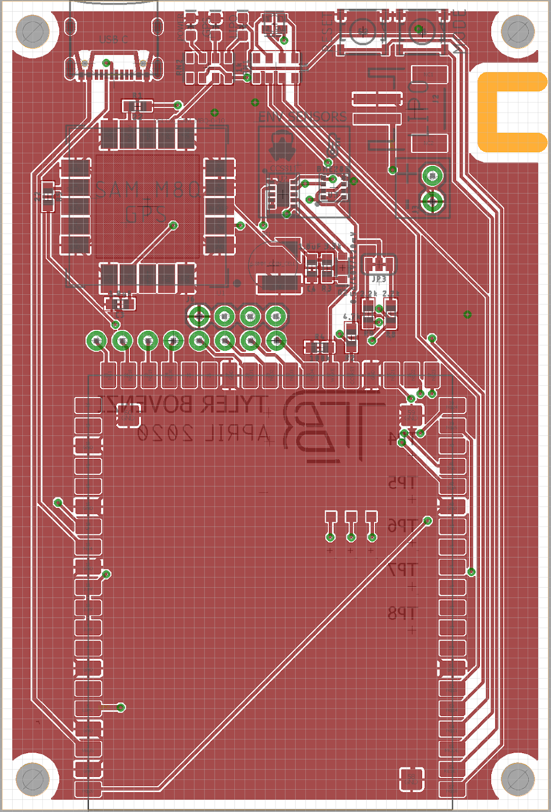
While designing the printed circuit board (PCB) that would house the components, I first came up with a rough structure for where parts should be located. The USB interfaces, indications LEDs, pushbutton switches, and battery connection are located on the front end of the top side of the PCB. In essence, everything the user interfaces with is in the same region of the board. The Particle E series controller board is on the back of the top side such that the castellated edge pins are more accessible to the rest of the board. Sensors and GPIO breakout headers are located in the middle. This helps prevent RF and thermal interference on the more sensitive components.
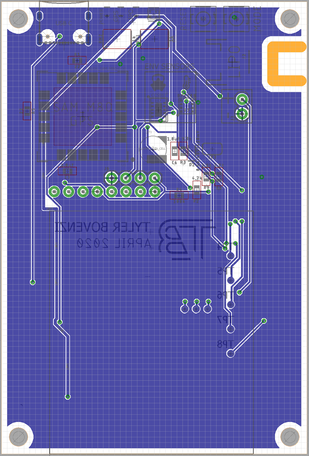
I designed the circuit board such that all components were mounted on the top side. While this was spatially inefficient, it simplifies assembly. Most resistors and capacitors use an 0603 form factor so it's crucial that the design allows reflow soldering. All components on the board are surface mount with the exception of the USB C mounting holes and optional pin header breakouts for GPIO expansion.
The yellow lines on the right side of the board indicate the desired milling area. I wanted to cut out this region to allow the lipo battery cable and antenna connection to come from below the board to their respective connectors. This made it possible to mount the PCB flush inside a case made to the exact dimensions of the edges of the board.
I also placed 3M holes on each corner of the board for future mounting and other applications.
I placed the lipo battery JST connector right next to the auxiliary power input. I also placed test pads on the bottom of the board to prevent cluttering on the top side.
Finally, there are a few icons on the board noting the air quality and temperature sensor, as well as my name and approximate date of design.
Top Layer
Bottom Layer (Mirrored)
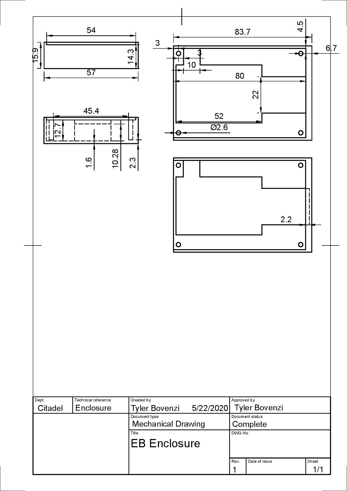
Enclosure
Design Process
In Fusion 360, I sketched the dimensions of the circuit board to design the enclosure around. I decided the board would sit on top of the box such that buttons and connectors were easily accessible. To accommodate this, I designed a box with an interior cavity to house the lipo battery and antenna.
To facilitate electrical connections between the top and bottom and what lies beneath it, I cut out a section to match the opening milled on the PCB. I also left holes to thread 3M screws. This eliminated the need for thread inserts or tapping.
The design documents included are the section version. I ended up creating a cut out such that the antenna could sit flat without extending the size of the enclosure. I printed the enclosure on a Creality Ender 3.
Below I’ve included some pictures of the enclosure as well as some figures to conceptualize its assembly:
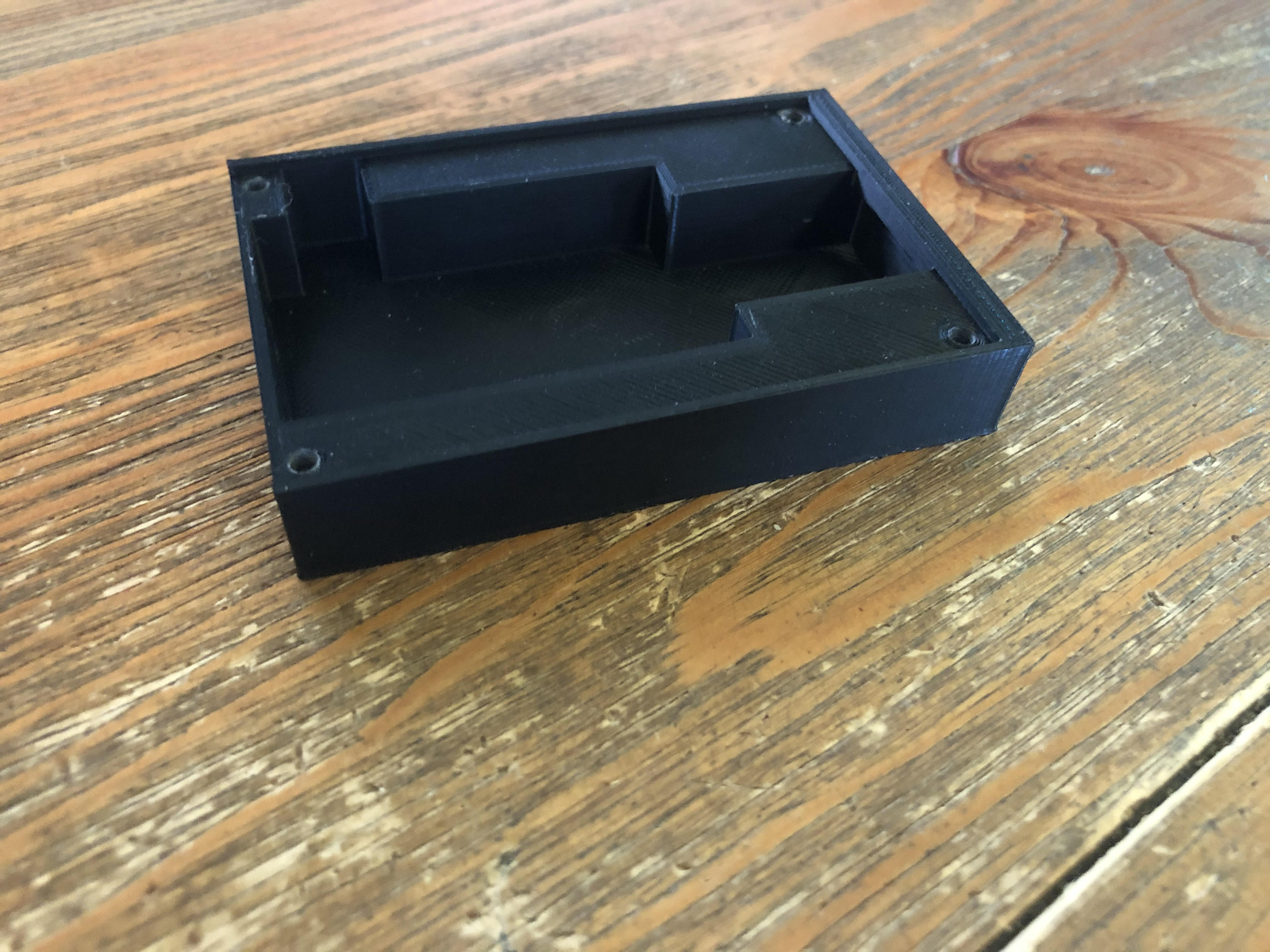
Component Layout within Enclosure

Side Profile with Enclosure Hidden

Assembly
Solder Application
I began assembly by attached extra blank PCBs to a flat board to create a well that held the target board in place. The stainless steel stencil came as a large unwieldy sheet. I used tin snips to cut it to size. I placed the target PCB in the jig and secured it with electrical tape. I lined up the pads on the board with the corresponding cut outs on the stencil and secured the stencil with more tape.
I applied a thin line of solder paste on top of the stencil and used a plastic card to evenly move the paste onto the pads. I repeated this process until there was a sufficient amount of solder paste on all solder pads. I then lifted the stencil to ensure no bridges were made that could prevent desired functionality down the road.
Component Placement
With solder paste already applied, I used tweezers to carefully place components on the board. I started with components of more complexity and difficulty, such that mistakes could be corrected without extensive backtracking. After placing a few of the integrated circuits, I moved to the smaller passive components. I used the relevant data sheets for components to ensure orientation and pinout were correct before putting them on the PCB.
Reflow Soldering
After the components had been placed, I was ready to reflow. I placed the PCB on a hot plate using foil to separate the two. I gradually increased heat to melt the solder paste while ensuring heat was low enough to prevent damage to components. The solder paste changed color from a dull gray to a bright silver, indicating that the components had been successfully connected. After a few minutes, all pads became shiny, indicating the process was complete. I then tested continuity with a multimeter before applying power to the circuit.
Repairs and initialization
Repairing USB data connection
Testing the functionality of the board revealed that all systems were functional except for USB data transmission and reception. After careful consideration of the schematic I determined there had been a wiring error where the top and bottom of the data were not connected. On top of this, D+ was connected to the top rail of the USB C connector, while the D- was connected to the negative rail. To fix this, I soldered a male pin header to D+ rail and connected the USB connector as normal. Using a custom cable allowed me to send and receive commands to and from the board. Below I have included a snippet of the flawed portion of the schematic as well as my temporary solution. This setup is not ideal, I plan on fixing this by either soldering the correct connection on the USB C connector, or remaking the PCB at a later date.
Initialization
Initializing the board required flashing code using the Particle command line interface. After being set up, the device can receive code via cellular communication. After installing particle drivers and API, I opened command prompt, connected the board to my computer, and typed particle setup. The software walked me through the steps, allowing me to log in, detect my device, and flash the basic pre-written code. I restarted the device and allowed the cellular modem to connect, as indicated by the steady cyan light.
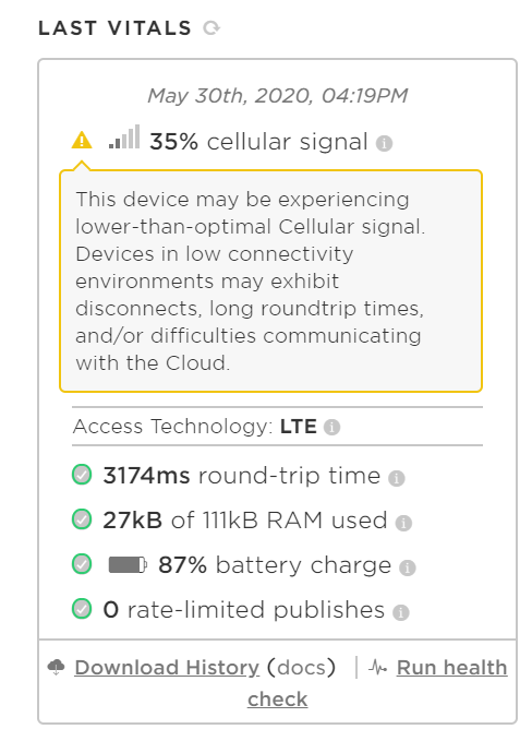
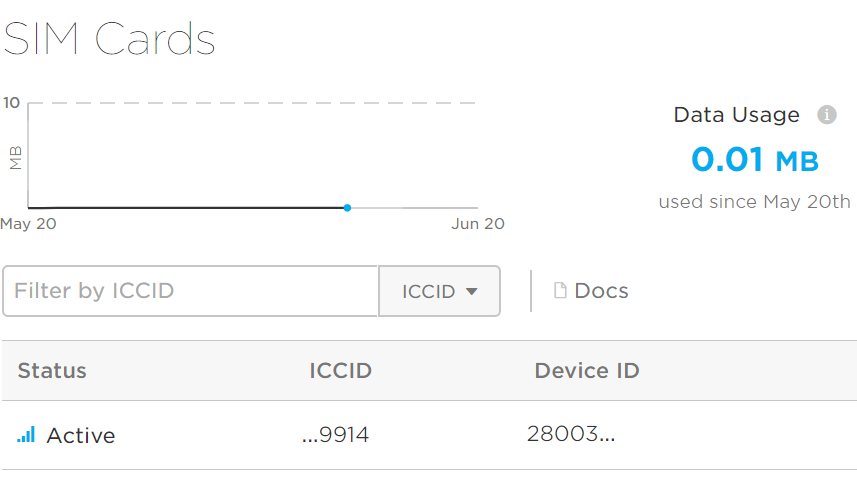
With the device connected I could manage vitals, view the events console, and monitor the device remotely through the browser based Particle console. I’ve included some of the sample interfaces from the console below.
Functionality
Board capabilities
With both the hardware and software completed and functional, the board has extensive capabilities. First, the device reads temperature, humidity, atmospheric pressure, and air quality to a high degree of precision. It does this by using recorded values to calibrate the sensors during operation. For example, the device uses temperature recording to better approximate the humidity readings.
Additionally, the SAM M8Q GPS provides geolocation data with accuracy of a few meters. This data is sent via I2C to microcontroller where it can be analyzed, time stamped, and posted remotely wherever necessary. The GPS IC takes a few minutes to lock on when indoors, and mere seconds without overhead obstructions. The backup battery allows the GPS to maintain satellite connectivity during hibernation states and restarts.
The Particle Electron Microcontroller handles power management. The Lipo battery can be charged during use both by the USB and auxiliary power connector. Typical battery life can range between a few days up to several weeks depending on power mode. The battery status is accessible via updates sent to the Particle Console.
The onboard cellular modem connects the device to the cloud. Similar to the GPS, locking on to reception can take anywhere from a few seconds to a few minutes depending on nearby obstructions and area signal strength. The cloud status is indicated on the board, and connectivity vitals can be acquired via the console as well.
Typical Usage
Currently, typical operation consists of the following:
- Connection to cellular network and GPS satellites
- Initialization of databases and connection to web servers
- Sensor calibration period
- Sensor data acquisition
- Update server with new geolocation and weather data
- Hibernation - Loop steps 4, 5, and 6
Adafruit Dashboard
I used adafruit.io to create a browser based dashboard for the device to send readings to. Recorded weather data is displayed on gauges with customizable ranges. I also wanted to see a history of temperature data. Temperature readings are displayed on a line graph that visualizes weather over time. Geolocation data is plotted on an interactive map. This connects each location reading, displaying the path taken.
The device sends MQTT updates to the dashboard. These updates are automatically displayed as soon as they come in. A list of updates containing timestamps is contained in the feed and accessible to project administrators.
Sensor Gauge Example

What I learned from the project
Over the course of the project I learned about component comparison, circuit design, PCB manufacturing, assembly, diagnostics, software engineering, and more.
Component Comparison was a very educational, yet time consuming process. For each of the IC’s I implemented in the final design, I spent several hours researching data sheets, reading forums, looking at circuit schematics, and comparing prices. This process allowed me to fully understand the functionality of each component and prevent any potential interfacing problems down the road.
Before this project, I had completed several other circuit design projects. These projects were basic, and involved inefficient layouts. Early projects also primarily consisted of through hole components. For this project, I wanted to make the board as dense and space efficient as possible. To do this, I researched SMD components and imported them to Eagle. I also manually placed components and routed traces to minimize complexity and optimize thermal performance.
When I started this project I was familiar with a soldering iron and had successfully soldered multiple through hole circuit boards. Surface mount assembly was a relatively new technique for me. I completed extensive research on this process and familiarized myself before attempting to assemble the real thing. The process worked on the first try, no components were damaged by the heating.
The device did not connect to my computer when I powered it on. I spent several hours trying to troubleshoot the connection. I wasn’t sure if there was a problem with my design, a driver issue, or simply a computer io error. I later traced the origin to a missing trace in the board design file and made a temporary fix. While writing the software, I used the serial monitor and events console to log internal processes in order to find semantic errors.
Writing device firmware that accomplished the requirements was no easy task. I encountered countless problems due to sensors interfering with one another. I later fixed this by allowing the device to switch through different modes that only used compatible sensors, while turning off others. I also found myself switching communication protocols over the course of the project. I learned that the basic webpage data library I was using was not compatible with the interactive map interface. As a result, I later switched to MQTT.
Outside of the Electrical Engineering skills I acquired from this project, I learned a lot about research and logistics. To reduce complexity, I tried to consolidate the bill of materials to as few distributors as possible. With the several distributors I ended up using, I also had to plan shipping. I even deemed several distributors unfeasible due to logistic timing or cost.